

History
October 03, 2014

Over the past decade, engineers working to create software-defined radio (SDR) systems have found it challenging to design a highly flexible wireless system that meets the military’s space, weight, and power (SWaP) requirements at an affordable cost.
The SDR sector received a major boost when the US Joint Tactical Radio System (JTRS) program was launched in 1997. The ambitious goal of the program was to enable mobile ad hoc networks to connect various wireless systems from the various branches of the military, other NATO armed forces, legacy radios and some civilian systems. To see also : What The US Military Is Learning About Jamming From The War In Ukraine. These systems include ground mobile radios (GMR), ground-to-air and satellite communications.
The JTRS specification included a wide range of so-called “waveforms” that would be modulated on any RF frequency over a huge range from high frequency (HF) to ultrahigh frequency (UHF). The physical layer of the specification included Orthogonal Frequency Division Multiplexing (OFDM) and Wideband Code Division Multiple Access (WCDMA) technologies to allow users to communicate via voice, data and video simultaneously at all levels of security. The system is designed to support the need for mobile command, control, communications, computing, intelligence, surveillance and reconnaissance (C4ISR) and maintain connectivity in the chaotic battlefield environment by using a self-healing network.
These technologies require complex baseband signal processing to realize the various waveforms. To achieve both processing speed and low power consumption, the design requires some form of hardware acceleration. The two most suitable options would be a wire mask, a programmable gate array, or field programmable logic such as a field programmable gate array (FPGA). The advantages of the “classic” gate matrix include optimized performance and low power; however, once the design is committed to silicone, it has permanently fixed functionality. Additionally, non-recurring engineering (NRE) costs have escalated dramatically for leading technologies due to the long production timelines typical of defense procurement. The FPGA option provided a flexible logic fabric; because it is reprogrammable, it allows design iterations to be tested in non-NRE hardware.
The RF challenges also proved to be very difficult. Designing an RF circuit that can cover a wide range of frequencies is far from easy, with different frequencies requiring adjustable components and a flexible antenna. The bandwidth required for voice is much narrower than that required for video, which complicated the design. Rapid frequency hopping, spread spectrum or OFDM further compounded the problems.
Unfortunately, the specification proved too complex and difficult for the technology of the day, and the JTRS program was finally canceled in late 2011. The program also suffered from feature creep and bloated requirements during its 15 years of development, which made much of from earlier work obsolete. When the cancellation of the program was announced, the Deputy Secretary of Defense was quoted as saying, “It is our assessment that the products resulting from the JTRS GMR development program are unlikely to affordably meet service requirements and may not at all do not meet some requirements. Termination is therefore necessary.
JTRS program elements live on
Fast forward to 2014: Many of the JTRS program requirements remain relevant today.
Moore’s Law progress is relentless, so FPGAs manufactured using 20-nm planar technology are currently shipping, with 14-nm Tri-Gate (FinFET) technology just around the corner. This update dramatically increased both complexity and performance. For example, the mid-range Altera Arria 10 SX family expands to 660k logic elements, along with well over 40 Mbits of on-board memory and more than 1k DSP accelerators. The 20-nm SX devices also feature dual high-performance ARM processors.
Question: How could a designer use an Arria 10 device to meet SDR baseband requirements? The first solution is to divide the tasks between the software running on the ARM processors and the hardware accelerators and interfaces that will be built into the logic structure. As a general rule, computationally intensive functions such as fast Fourier transform (FFT) or error correction (FEC) encoding and decoding are usually more efficient in hardware. The CPU is ideal for activities such as moving data into memory and checking and manipulating protocols.
The equivalent of baseband “waveforms” would be different modulation standards. These can be OFDM, which requires complex FFT calculations, or Code Division Multiple Access (CDMA), requiring fast spreading code generation and correlators to reduce and recover the received data. The DSP blocks in the Arria device form a key element of the hardware accelerator. Modern modulation systems use data in the form of in-phase (I) and quadrature (Q) bit streams; this allows the RF carrier to be modulated with quadrature amplitude modulation (QAM) such as 16 (up to 256 QAM) or the simpler quadrature phase keying (QPSK). This high-performance task can be implemented in the DSP and logic structure to save overall system power.
The latest standard is called Multiple-Input Multiple-Output (MIMO), a complex scheme that uses two or more antennas separated by a physical distance. MIMO techniques improve spectral efficiency and achieve diversity gain, which improves link reliability. MIMO is expected to become an important addition to meet the growing demand for data throughput.
A programmable logic solution offers significant additional benefits. The logic function is defined by a configuration file stored in non-volatile external memory and loaded into the device at power-up; the memory also contains the executable code for the ARM cores. This solution allows the functionality to be updated as a mid-life software update, as users could for example support new waveforms in the logic or add new features to the ARM code.
ARM processors can control the flow of data into the FPGA cores by using them as custom peripherals. As an example, one core can be allocated to manage interfaces, such as a display or video screen, while checking that the received data packets are valid (see Figure 1). The second processor can manage the hardware accelerators built from the logic and DSP resources. ARM can choose the hardware accelerators that perform the algorithm currently needed, for example to produce QAM16 and to regulate data transfer to and from the field programmable radio frequency (FPRF) chip.
Figure 1: FPGA controlling the SDR logic.
(Click on graphic to enlarge)
|
|
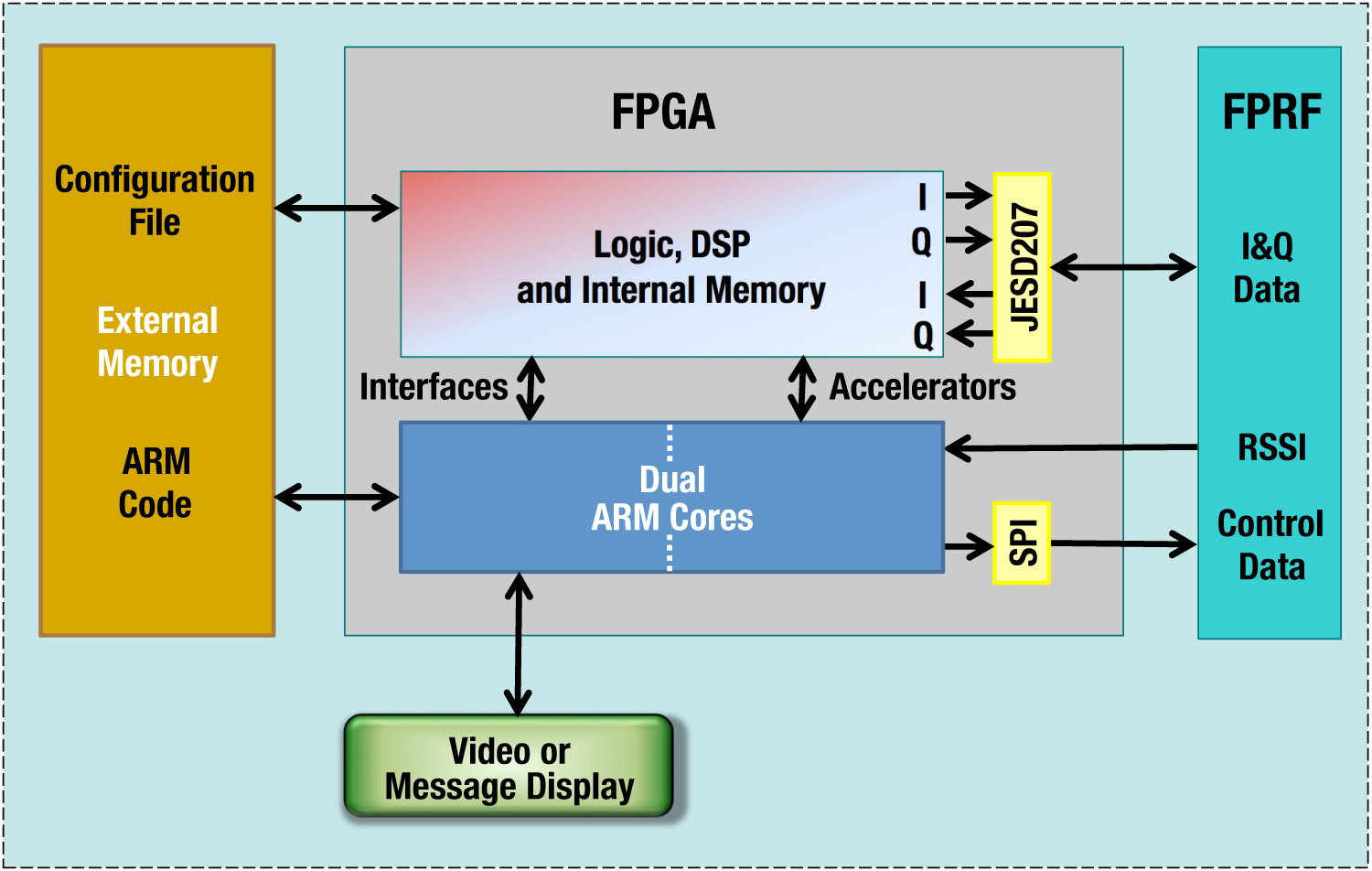
ARM can also drive the FPRF device with a simple and fast SPI interface using a two-byte instruction to give it full control over the RF domain. The processor can also process the resulting Signal Strength Indicator (RSSI), which indicates the level of activity on the selected frequency. The combination of FPGA and FPRF devices provides an extremely flexible, low-power and above all cost-effective solution for the logic and RF domains.
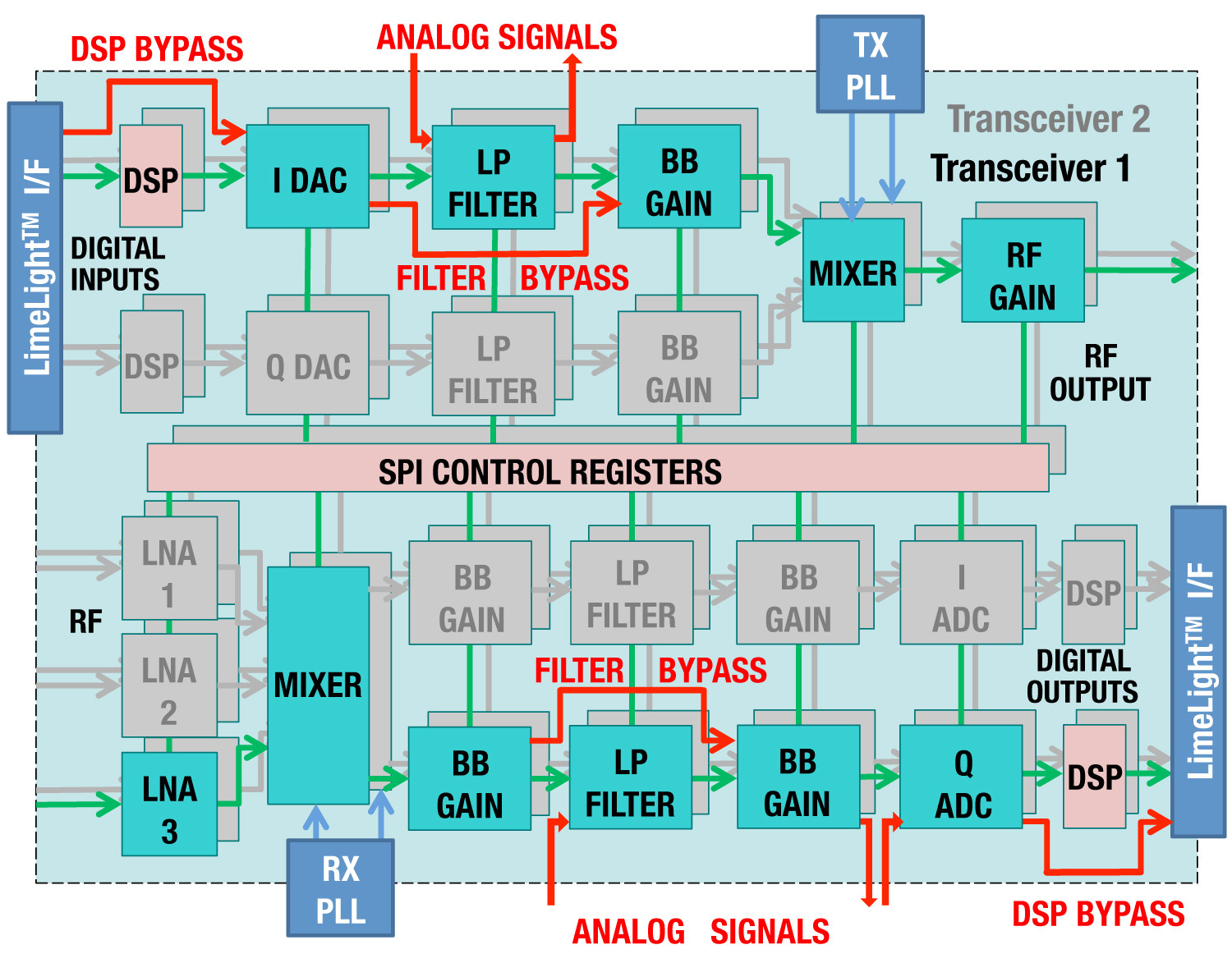
The LMS7002M, the second generation FPRF device from Lime Microsystems, is a recently announced 65-nm CMOS chip that features a dual transceiver architecture. The frequency range has been extended so that it now covers 50 MHz to 3800 MHz, providing support for the lower frequencies often used in legacy military radios. In addition, the upper limit can be easily extended with the addition of an external PLL and mixer so that it can cover the frequencies used in satellite communications.
The LMS7002M includes an on-chip microcontroller; this setup simplifies on-chip calibration that would otherwise involve complex interactions with baseband logic. It calibrates the DC offset, TX/RX LPF bandwidth tuning, local oscillator leakage transmission, gain and phase mismatch in the transmit and receive circuits, and on-chip resistor and capacitor handling. In most applications, initial calibration is sufficient; however, for military wireless systems operating at extreme temperatures and frequencies, the microcontroller can be instructed to recalibrate to ensure optimal performance. Power-saving features include the ability to selectively turn off each block when not needed, with settings and calibrations preserved if power to the SPI memory is maintained (see Figure 2). The FPRF chip is housed in an 11.5mm x 11.5mm package.
Figure 2: Each FPRF block can be selectively disabled or skipped.
(Click on graphic to enlarge)
|
|
Various tools are available to assist designers, provided by the FPGA vendor or third-party vendors. For example, Altera is the only FPGA vendor that offers a publicly available Open Computing Language (OpenCL) compliant software development kit. OpenCL allows programmers to take OpenCL code and quickly use the massively parallel architecture of FPGAs. It enables emulation and debugging of kernel code, detects performance bottlenecks, and profiles and recompiles to a hardware implementation. The FPRF design tool from Lime Microsystems is in the form of a graphical user interface (GUI); The GUI is available for free and allows full control of the device.
Paul Dillion has worked with Lime Microsystems covering a range of marketing projects for the past two years. He previously worked in the FPGA industry for 15 years and authored The FPGA Market report. Paul has worked in strategic and tactical marketing roles for leading semiconductor companies in the US and UK and specializes in competitive analysis and negotiations. Readers can find it at [email protected].
Lime Microsystems
630-208-2700
www.limemicro.com
Featured companies

Comments are closed.